「第22回 半導体・センサ パッケージング技術展」に出展いたします
来る2021年1月20日(水)より、東京ビックサイトにて開催されます「第22回 半導体・センサ パッケージング技術展」へ出展致します。
ご来場の際はぜひ弊社ブースへお越しください。 皆さまのご来場を、心よりお待ちしております。
無料ご招待券をご用意致しましたので、ご希望のお客様は下記フォームよりお申込みください。
※枚数に限りがございますので、お早めにお申し込みください。
ご来場の際はぜひ弊社ブースへお越しください。 皆さまのご来場を、心よりお待ちしております。
無料ご招待券をご用意致しましたので、ご希望のお客様は下記フォームよりお申込みください。
※枚数に限りがございますので、お早めにお申し込みください。
| 開催期間 / Dates |
2021年1月20日(水)~22日(金)10:00~18:00(最終日のみ17:00まで) January 20 (Wed) - 22 (Fri), 2021 10:00-18:00 (Last day until 17:00). |
|---|---|
| 会場 / Venue | 東京ビックサイト / Tokyo Big Sight, Japan |
| ブースNo. / Booth Number | 西2ホール W11-12(「(株)東京精密」ブース内) / West Hall 2 W11-12 |
| 入場料 / Register | 5,000円※招待券持参者は無料 / JPY 5,000/person will be charged without a ticket. |
| 公式URL / Official URL | https://www.icp-expo.jp/ja-jp.html |
注目の出展製品
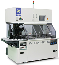
ウェーハ面取り機 / Wafer Edge Grinding Machine
SiC, GaN, GaAs 等様々な材料・形状加工を提供いたします
Technology Solutions for Wide Range of Needs in EDGE Grinding Process
Technology Solutions for Wide Range of Needs in EDGE Grinding Process
近年、ウェーハの品質向上の要求が強く、ウェーハ端面(エッジ部)の加工状態が重要視されております。
シリコン、サファイア、SiCなど多種材料のウェーハ外周部面取りを行う加工機「W-GMシリーズ」。Siメーカーのみならず、化合物半導体、酸化物材料メーカーなど多方面にわたって高い評価を受けております。
シリコン、サファイア、SiCなど多種材料のウェーハ外周部面取りを行う加工機「W-GMシリーズ」。Siメーカーのみならず、化合物半導体、酸化物材料メーカーなど多方面にわたって高い評価を受けております。
The requirement for the wafer quality is getting higher and the condition of wafer edge is getting more important.
The edge grinders “W-GM series” process edge grinding of various kind of materials such as Silicon, sapphire and SiC.As a solution for that, Our W-GM series are highly rated among manufactures of silicon, compound materials and other wafer shaped materials.
The edge grinders “W-GM series” process edge grinding of various kind of materials such as Silicon, sapphire and SiC.As a solution for that, Our W-GM series are highly rated among manufactures of silicon, compound materials and other wafer shaped materials.
<EDGE面取りプロセス導入による5つのメリット / 5 ADVANTAGES>
-
搬送時のチッピングによるワレ・カケを低減
Protects the wafer edge from chipping and breaking -
加工プロセスの短縮、ランニングコストの減少
Shorten the process step and reduce running cost -
コインマークレス、クラック減少、ウェーハエッジ上の膜等不要箇所の除去
Improves quality, coin markless, crack reduction, removes defective area on wafer edge -
ナイフエッジ防止
Prevents sharp knife edge -
次の工程の為の様々なエッジ形状、高精度 Notch 形状、OF の成形
Changes edge shape for the following process and accurate Notch / OF shape
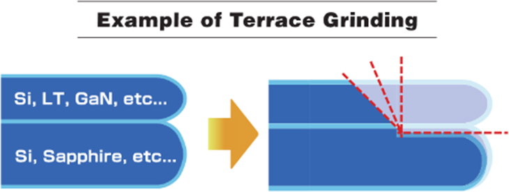
トリミング加工編 / Edge Trimming
自動車の運転などに使用する微小センサ―MEMSや、4G5Gスマートフォンに
用いる通信向けSAWデバイスの需要が高まっています。
これらのデバイスを製造するために必要なプロセスにウェーハ接合プロセスがありますが、接合後のウェーハ薄化プロセスで端面からの発塵やクラックなどが問題視されています。これらの対策としてエッジのテラス加工プロセスがあります。
The demand for MEMS used for automotive and SAW device used for 4G5G smartphones is increasing.
The wafer bonding process is needed for making those devices though,the problems are the vibration and crack from the wafer edge in the thinning process after the bonding process.
Our edge trimming (terrace grinding) process can be the solution for those problems.
The wafer bonding process is needed for making those devices though,the problems are the vibration and crack from the wafer edge in the thinning process after the bonding process.
Our edge trimming (terrace grinding) process can be the solution for those problems.
弊社エッジトリミング加工では、LiNBO3/シリコン、サファイア/シリコン、石英ガラス/シリコン、
LiTaO3/シリコン、LiTaO3/サファイア、LiTaO3/水晶、SOIウェーハなど様々な種類に
対応しております。任意の角度に加工することが可能です。
Our edge trimming (terrace grinding) process is capable with various materials such as LiNBO3 on Si, Sapphire on Si, Quartz on Si, LiTaO3 on Si, LiTaO3 on Sapphire, LiTaO3 on Quartz, and SOI wafers.
The trimming angle can be designed based on your demand.
・対応サイズ:Φ100mm~Φ300mm 厚さ400μm~1500μm
The trimming angle can be designed based on your demand.